Поделиться

Semiconductor Materials
Semiconductor Materials
The Semiconductor Industry
Semiconductor devices such as diodes, transistors and integrated circuits can be found everywhere in our daily lives, in Walkman, televisions, automobiles, washing machines and computers. We have come to rely on them and increasingly have come to expect higher performance at lower cost.
Personal computers clearly illustrate this trend. Anyone who wants to replace a three to five year old computer finds that the trade-in value of his (or her) computer is surprising low. On the bright side, one finds that the complexity and performance of the today’s personal computers vastly exceeds that of their old computer and that for about the same purchase price, adjusted for inflation.
While this economic reality reflects the massive growth of the industry, it is hard to even imagine a similar growth in any other industry. For instance, in the automobile industry, no one would even expect a five times faster car with a five times larger capacity at the same price when comparing to what was offered five years ago. Nevertheless, when it comes to personal computers, such expectations are very realistic.
The essential fact which has driven the successful growth of the computer industry is that through industrial skill and technological advances one manages to make smaller and smaller transistors. These devices deliver year after year better performance while consuming less power and because of their smaller size they can also be manufactured at a lower cost per device.
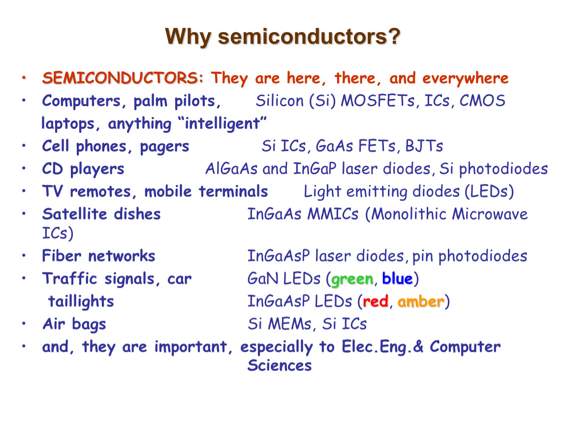
Why semiconductors?
SEMICONDUCTORS: They are here, there, and everywhere

Introduction
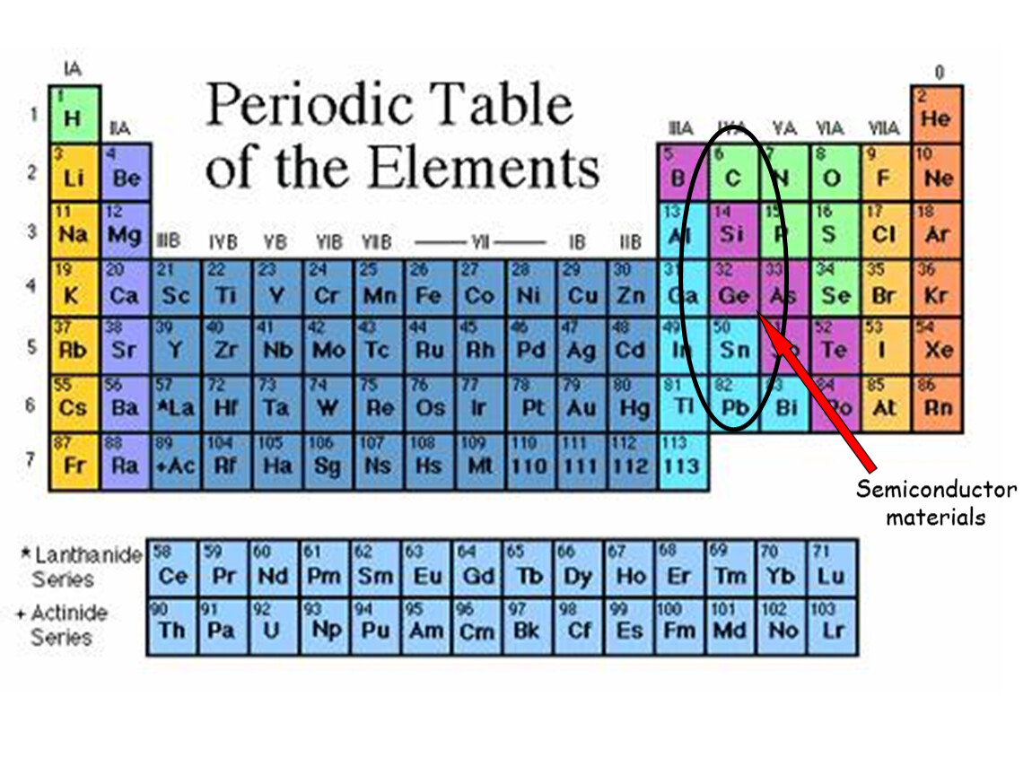
Semiconductors are materials whose electrical properties lie between Conductors and Insulators.
Ex : Silicon and Germanium
Give the examples of Conductors and Insulators!
Difference in conductivity
Semiconductor Materials
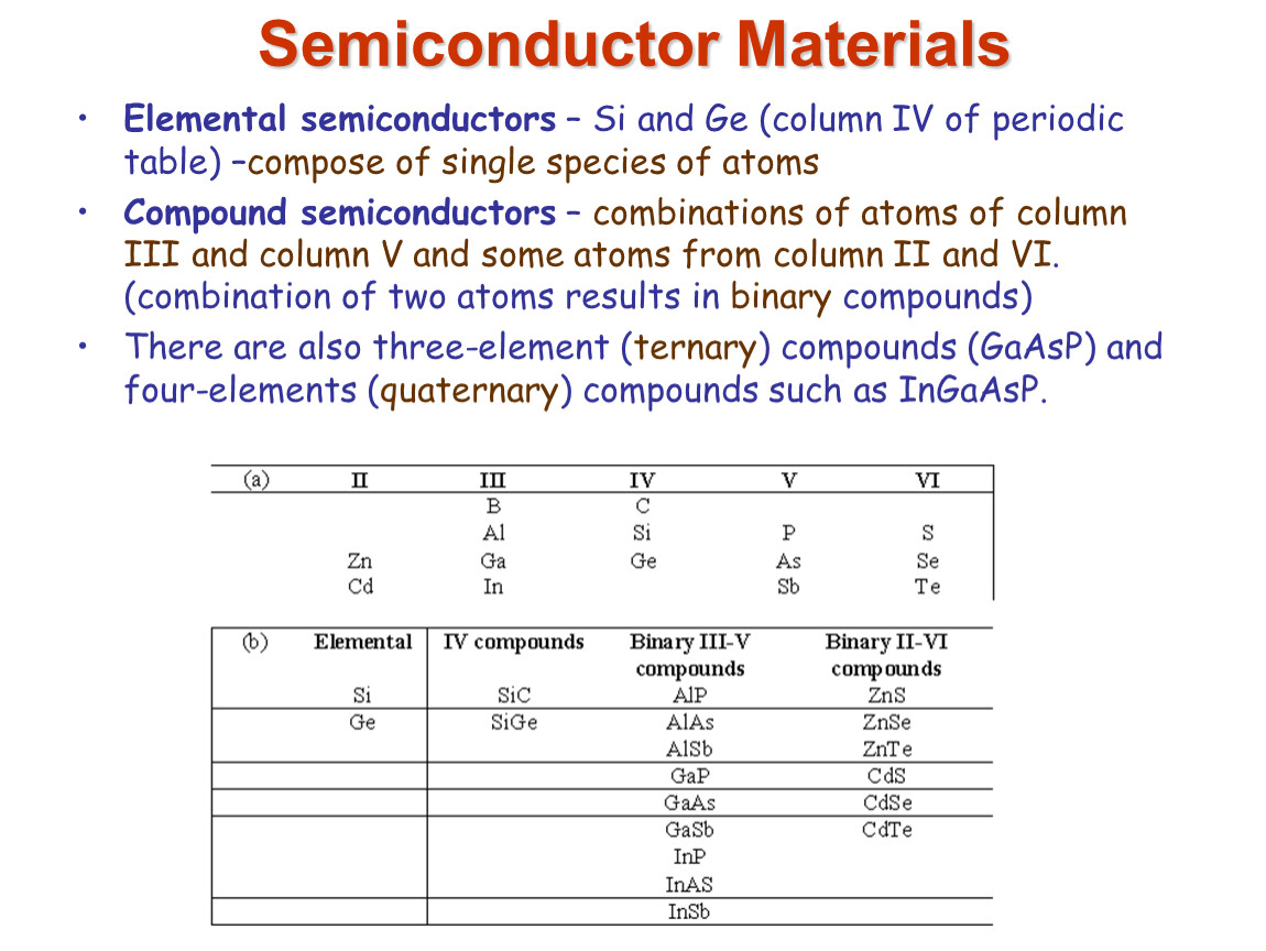
Elemental semiconductors – Si and Ge (column IV of periodic table) –compose of single species of atoms
Compound semiconductors – combinations of atoms of column III and column V and some atoms from column II and VI. (combination of two atoms results in binary compounds)
There are also three-element (ternary) compounds (GaAsP) and four-elements (quaternary) compounds such as InGaAsP.
Semiconductor materials
Semiconductor Materials
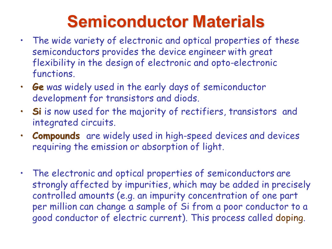
The wide variety of electronic and optical properties of these semiconductors provides the device engineer with great flexibility in the design of electronic and opto-electronic functions.
Ge was widely used in the early days of semiconductor development for transistors and diods.
Si is now used for the majority of rectifiers, transistors and integrated circuits.
Compounds are widely used in high-speed devices and devices requiring the emission or absorption of light.
The electronic and optical properties of semiconductors are strongly affected by impurities, which may be added in precisely controlled amounts (e.g. an impurity concentration of one part per million can change a sample of Si from a poor conductor to a good conductor of electric current). This process called doping.
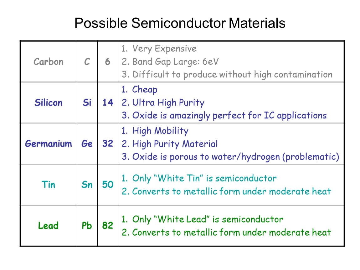
Possible Semiconductor Materials
Carbon | C | 6 | Very Expensive |
Silicon | Si | 14 | Cheap |
Germanium | Ge | 32 | High Mobility |
Tin | Sn | 50 | Only “White Tin” is semiconductor |
Lead | Pb | 82 | Only “White Lead” is semiconductor |
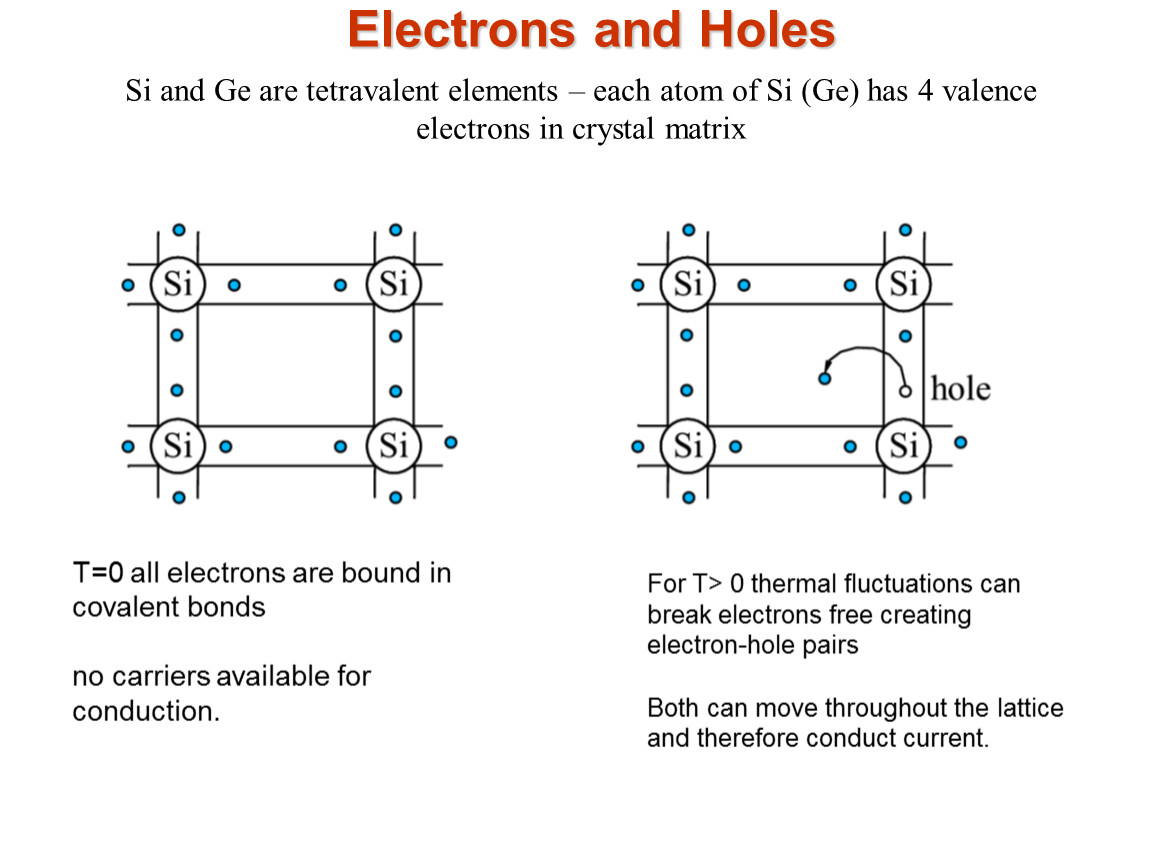
Si and Ge are tetravalent elements – each atom of Si (Ge) has 4 valence electrons in crystal matrix
T=0 all electrons are bound in covalent bonds no carriers available for conduction.
For T> 0 thermal fluctuations can break electrons free creating electron-hole pairs Both can move throughout the lattice and therefore conduct current.
Electrons and Holes
Electrons and Holes
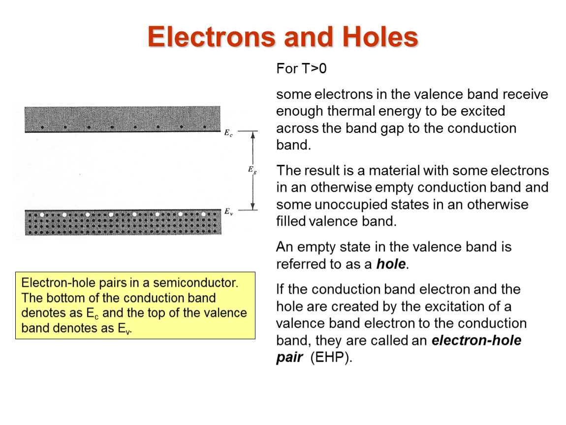
Electron-hole pairs in a semiconductor. The bottom of the conduction band denotes as Ec and the top of the valence band denotes as Ev.
For T>0
some electrons in the valence band receive enough thermal energy to be excited across the band gap to the conduction band.
The result is a material with some electrons in an otherwise empty conduction band and some unoccupied states in an otherwise filled valence band.
An empty state in the valence band is referred to as a hole.
If the conduction band electron and the hole are created by the excitation of a valence band electron to the conduction band, they are called an electron-hole pair (EHP).
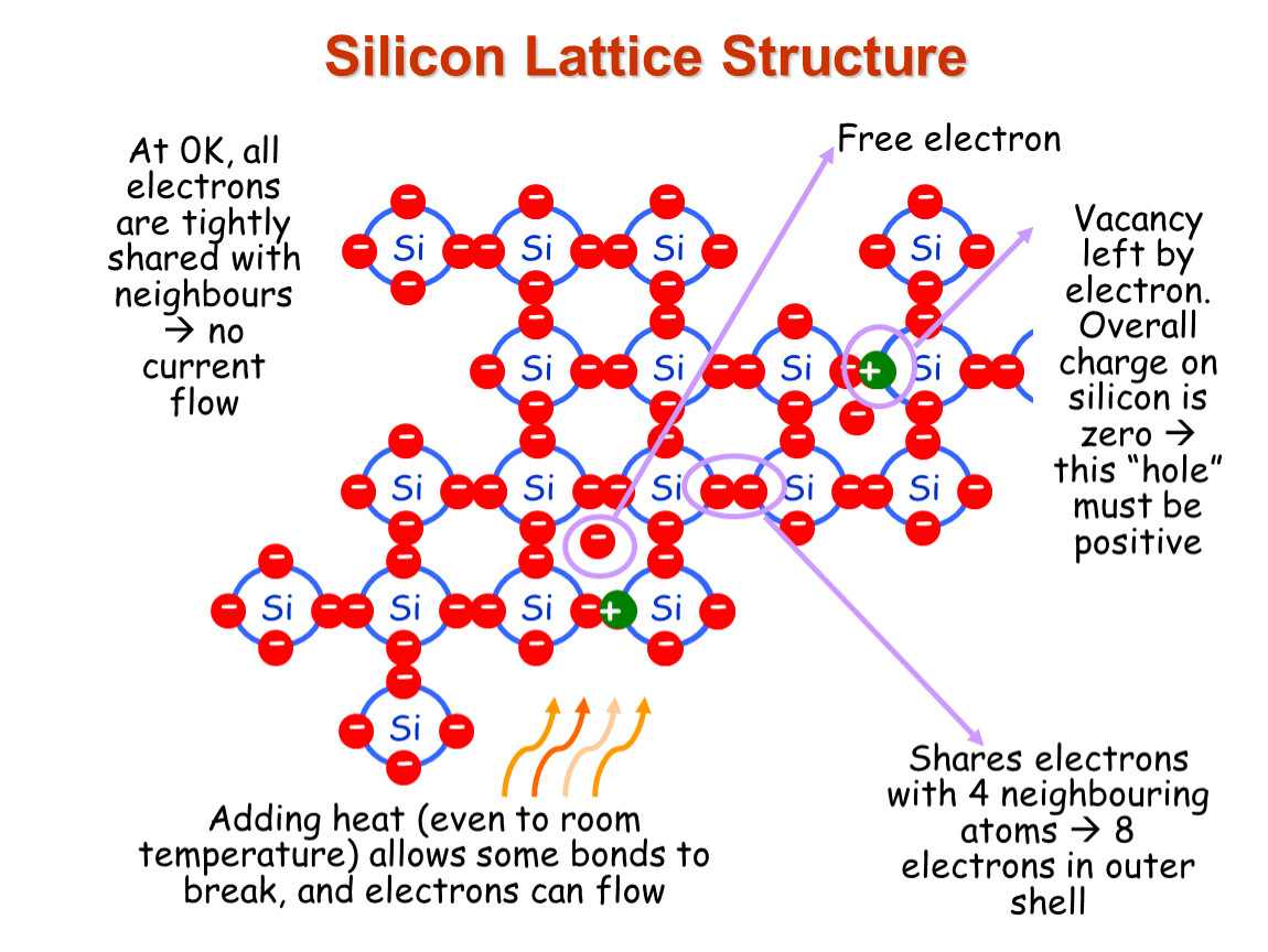
Silicon Lattice Structure
At 0K, all electrons are tightly shared with neighbours no current flow
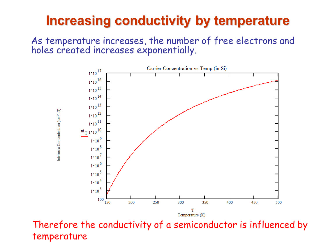
Increasing conductivity by temperature
Therefore the conductivity of a semiconductor is influenced by temperature
As temperature increases, the number of free electrons and holes created increases exponentially.
The conductivity of the semiconductor material increases when the temperature increases.
This is because the application of heat makes it possible for some electrons in the valence band to move to the conduction band.
Obviously the more heat applied the higher the number of electrons that can gain the required energy to make the conduction band transition and become available as charge carriers.
This is how temperature affects the carrier concentration.
Another way to increase the number of charge carriers is to add them in from an external source.
Doping or implant is the term given to a process whereby one element is injected with atoms of another element in order to change its properties.
Semiconductors (Si or Ge) are typically doped with elements such as Boron, Arsenic and Phosphorous to change and enhance their electrical properties.
Increasing conductivity
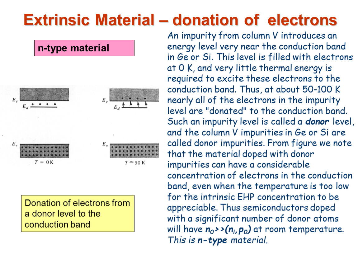
Extrinsic Material – donation of electrons
An impurity from column V introduces an energy level very near the conduction band in Ge or Si. This level is filled with electrons at 0 K, and very little thermal energy is required to excite these electrons to the conduction band. Thus, at about 50-100 K nearly all of the electrons in the impurity level are "donated" to the conduction band. Such an impurity level is called a donor level, and the column V impurities in Ge or Si are called donor impurities. From figure we note that the material doped with donor impurities can have a considerable concentration of electrons in the conduction band, even when the temperature is too low for the intrinsic EHP concentration to be appreciable. Thus semiconductors doped with a significant number of donor atoms will have n0>>(ni,p0) at room temperature. This is n-type material.
Donation of electrons from a donor level to the conduction band
n-type material
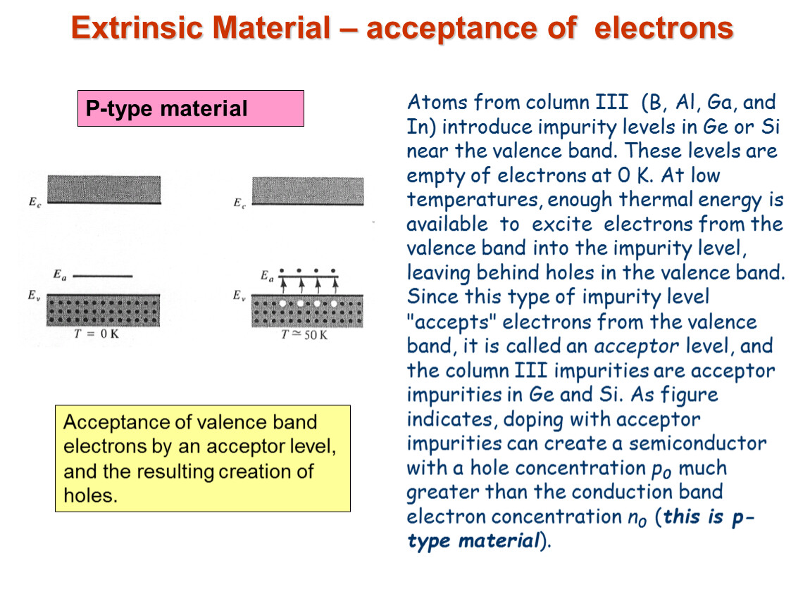
Extrinsic Material – acceptance of electrons
Acceptance of valence band electrons by an acceptor level, and the resulting creation of holes.
Atoms from column III (B, Al, Ga, and In) introduce impurity levels in Ge or Si near the valence band. These levels are empty of electrons at 0 K. At low temperatures, enough thermal energy is available to excite electrons from the valence band into the impurity level, leaving behind holes in the valence band. Since this type of impurity level "accepts" electrons from the valence band, it is called an acceptor level, and the column III impurities are acceptor impurities in Ge and Si. As figure indicates, doping with acceptor impurities can create a semiconductor with a hole concentration p0 much greater than the conduction band electron concentration n0 (this is p-type material).
P-type material
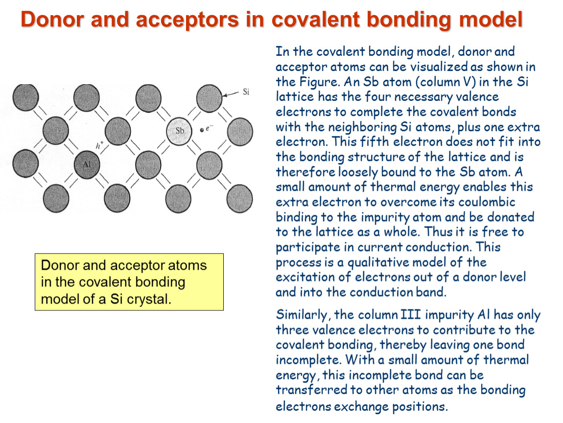
Donor and acceptors in covalent bonding model
In the covalent bonding model, donor and acceptor atoms can be visualized as shown in the Figure. An Sb atom (column V) in the Si lattice has the four necessary valence electrons to complete the covalent bonds with the neighboring Si atoms, plus one extra electron. This fifth electron does not fit into the bonding structure of the lattice and is therefore loosely bound to the Sb atom. A small amount of thermal energy enables this extra electron to overcome its coulombic binding to the impurity atom and be donated to the lattice as a whole. Thus it is free to participate in current conduction. This process is a qualitative model of the excitation of electrons out of a donor level and into the conduction band.
Similarly, the column III impurity Al has only three valence electrons to contribute to the covalent bonding, thereby leaving one bond incomplete. With a small amount of thermal energy, this incomplete bond can be transferred to other atoms as the bonding electrons exchange positions.
Donor and acceptor atoms in the covalent bonding model of a Si crystal.
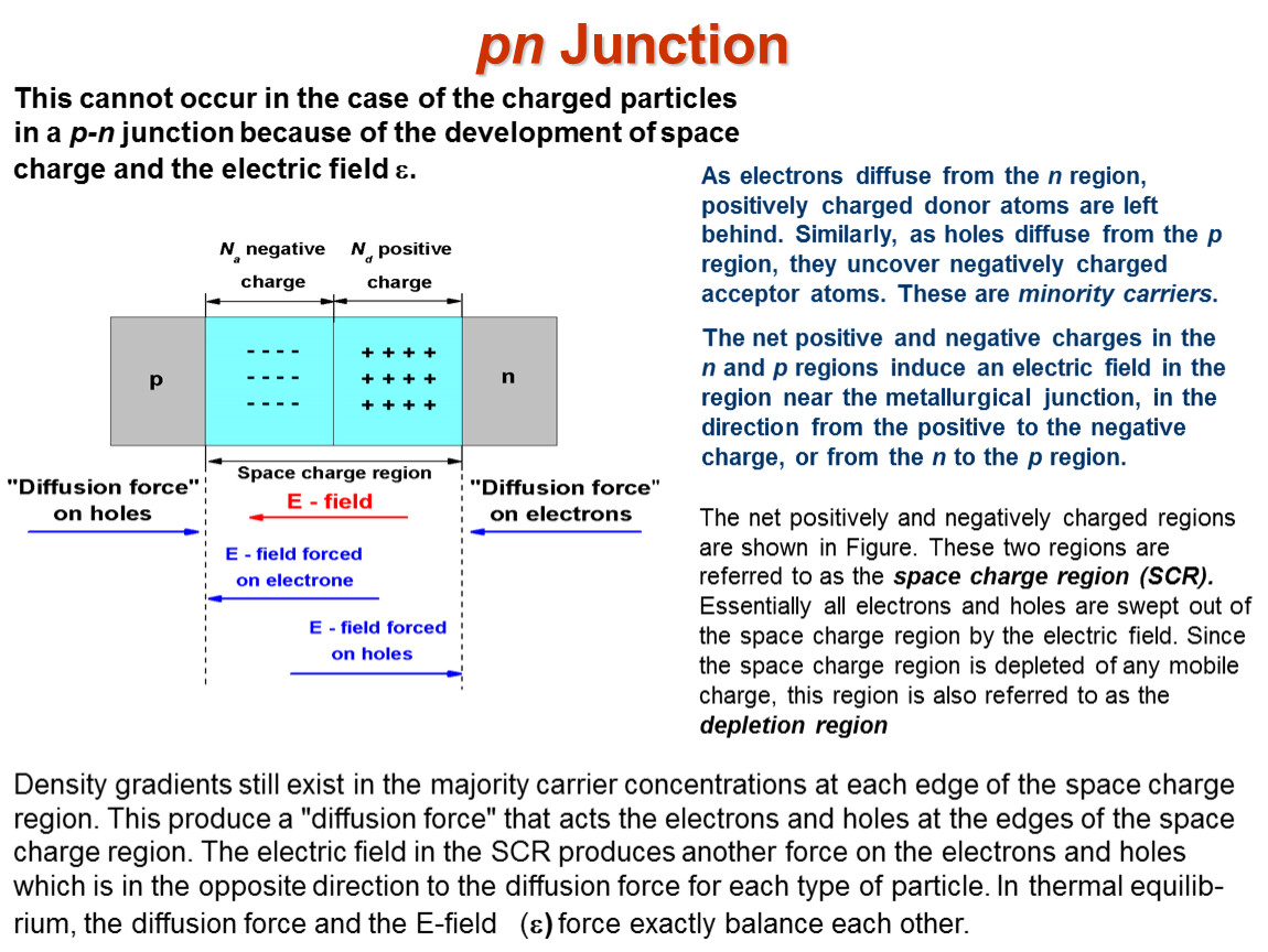
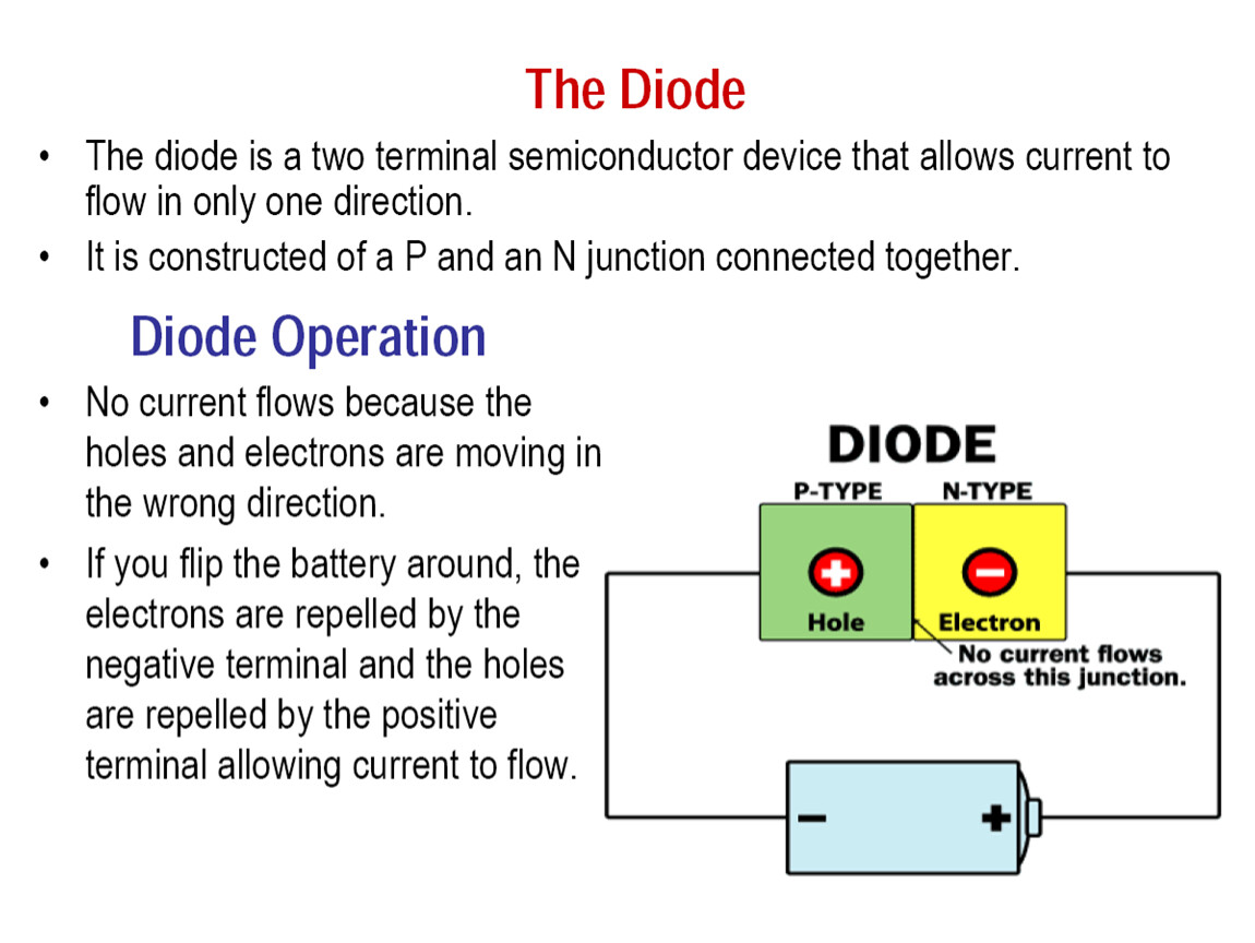
pn Junction
This cannot occur in the case of the charged particles in a p-n junction because of the development of space charge and the electric field .
As electrons diffuse from the n region, positively charged donor atoms are left behind. Similarly, as holes diffuse from the p region, they uncover negatively charged acceptor atoms. These are minority carriers.
The net positive and negative charges in the n and p regions induce an electric field in the region near the metallurgical junction, in the direction from the positive to the negative charge, or from the n to the p region.
The net positively and negatively charged regions are shown in Figure. These two regions are referred to as the space charge region (SCR). Essentially all electrons and holes are swept out of the space charge region by the electric field. Since the space charge region is depleted of any mobile charge, this region is also referred to as the depletion region
Density gradients still exist in the majority carrier concentrations at each edge of the space charge region. This produce a "diffusion force" that acts the electrons and holes at the edges of the space charge region. The electric field in the SCR produces another force on the electrons and holes which is in the opposite direction to the diffusion force for each type of particle. In thermal equilibrium, the diffusion force and the E-field () force exactly balance each other.
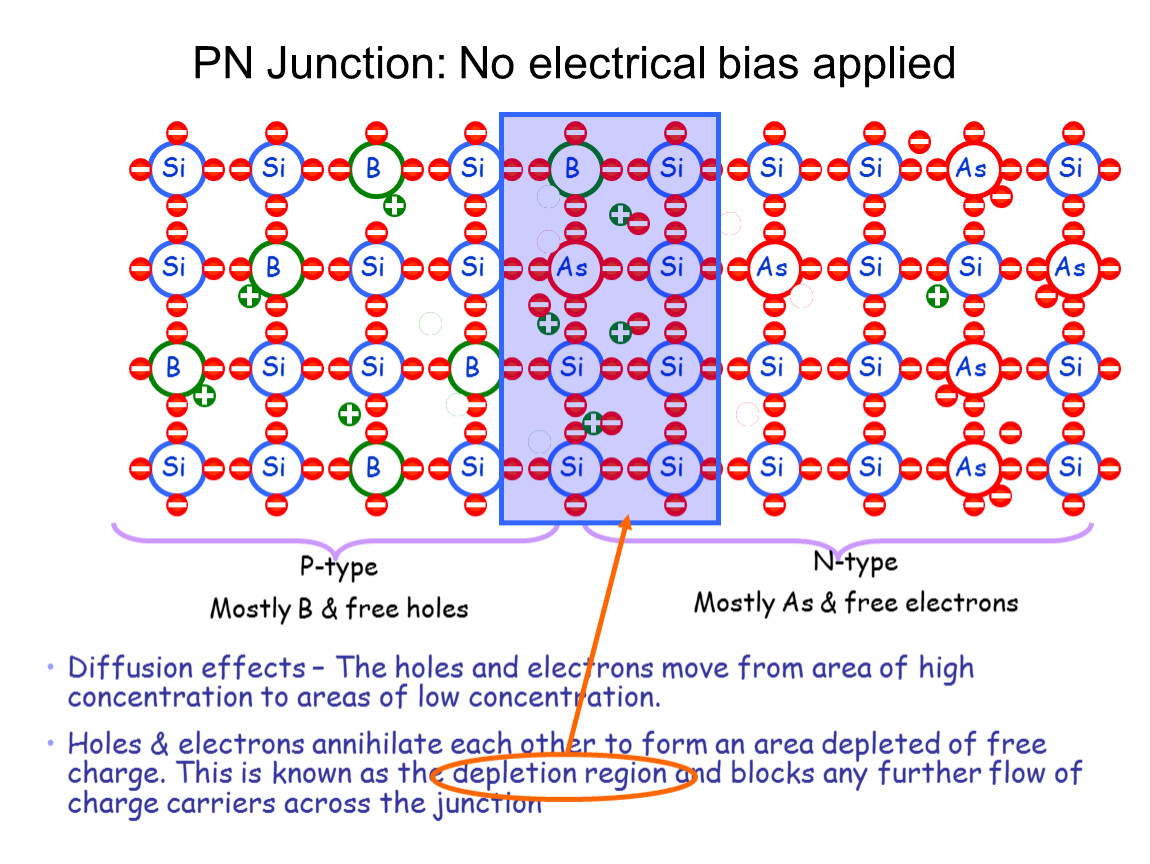
PN Junction: No electrical bias applied
Si
Si
Si
B
Si
Si
B
Si
Si
As
Si
Si
Si
B
Si
As
Si
B
B
Si
Si
B
Si
Si
Si
Si
Si
Si
Si
Si
Si
Si
Si
As
As
As
As
Si
Si
Si
N-type
Mostly As & free electrons
Diffusion effects – The holes and electrons move from area of high concentration to areas of low concentration.
Holes & electrons annihilate each other to form an area depleted of free charge. This is known as the depletion region and blocks any further flow of charge carriers across the junction
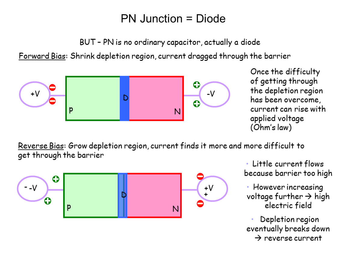
PN Junction = Diode
BUT – PN is no ordinary capacitor, actually a diode
Forward Bias: Shrink depletion region, current dragged through the barrier
Once the difficulty of getting through the depletion region has been overcome, current can rise with applied voltage (Ohm’s law)
Reverse Bias: Grow depletion region, current finds it more and more difficult to get through the barrier
Little current flows because barrier too high
However increasing voltage further high electric field
Depletion region eventually breaks down reverse current
-
+
Материалы на данной страницы взяты из открытых источников либо размещены пользователем в соответствии с договором-офертой сайта. Вы можете сообщить о нарушении.