Поделиться

READING TASK 1: APPLICATIONS OF SEMICONDUCTORS
These days with the rise of very large scale integration(VLSI) technology the transistors, which are the building blocks of memory chips ,can be made as tiny as in the scale of nano meter which allows us to fit millions of them into a small area. And the building blocks of these transistors are semiconductors.
Semiconductors find wide range of application in modern day gadgets. In fact if you observe carefully you are surrounded by semiconductors. The cell phone you use or the laptop has millions of tiny transistors embedded in them in order to empower them with various functionalities. The LED which is aggressively replacing many of the existing lighting technologies is a semiconductor device.
++++++++++++++++++++++++++++++++++++++++++++++++++++++++++++++
Semiconductor devices have number of applications. Some of the important applications of semiconductor devices are described in this section.
i) P-N Junction Diode as a Rectifier
The function of a rectifier circuit is that to convert a.c signal to d.c signals using p-n junction diodes. The peculiarity of a p-n junction diode is that it conduct only in one direction. If a diode is in forward biased condition, it will conduct, otherwise it will not. If a pulsating a.c signal is applied to the diode, only during positive half cycle it will conduct. Thus p-n junction diode subjected to an a.c voltage acts as a rectifier converting alternating voltage to a pulsating d.c voltage.
ii) Transistor as an Amplifier
Transistor is a three terminal device: Base, emitter and collector, can be operated in three configurations common base, common emitter and common collector. According to configuration it can be used for voltage as well as current amplification. The input signal of a small amplitude is applied at the base to get the magnified output signal at the collector. Thus provides an amplification of the signal. The amplification in the transistor is achieved by passing input current signal from a region of low resistance to a region of high resistance. This concept of transfer of resistance has given the name TRANSfer- resISTOR (TRANSISTOR).
Common Emitter Configuration:
As shown in figure, in this configuration input is applied between base and emitter, and output is taken from collector and emitter. Here, emitter of the transistor is common to both, input and output circuits and hence the name common emitter configuration. Common emitter configurations for both n-p-n and p-n-p transistors are shown in figure and 1 and 2 respectively.
iii) Transistor as a Switching Device
One of the very important applications of a BJT (bipolar junction transistor) is its use as a switching device for the computer logic circuits. The circuit shown in the figure can be used as a switch by proper selection of resistances. The transistor is made to operate in the two extreme modes, that is it operates either in the cut off or saturation mode. Consider an input signal shown in figure b applied at the input of the circuit in the figure a. When input Vin = -V1, transistor is designed to operate in cut off state by proper choice of RB, RC. Now IC is close to zero, therefore the output voltage V0 = VCC as shown in figure c. For Vin = V2, transistor goes into saturation or is driven 'ON'. When a transistor is biased in saturation region, we know that VCE = VCEsat. So that the output voltage V0 = VCEsat = 0.2 V. Thus, the output voltage is either high (= VCC for transistor OFF) or low (= 0 V for transistor ON). So, the circuit is indeed working as a switch.
Logic Gates and Their Realization
Logic gates are the basic elements that make up a digital system. The electronic gaate is a circuit that is able to operate on a number of binary inputs in order to perform a particular logical function. The types of gates available are the AND, OR, NOT, NAND, NOR, XOR and XNOR. The gate is a digital circuit with one or more input voltages but only one output voltage. By connecting the different gates in different ways, we can build circuits that perform arithmetic and other functions associated with the human brain because they simulate mental processes. The operation of a logic gate can be easily understood with the help of truth table. A truth table is a table that shows all the input-output possibilities of a logic circuit; that is the truth table indicates the outputs for different possibilities of the inputs.
READING TASK 2: INTRINSIC SEMICONDUCTOR
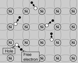
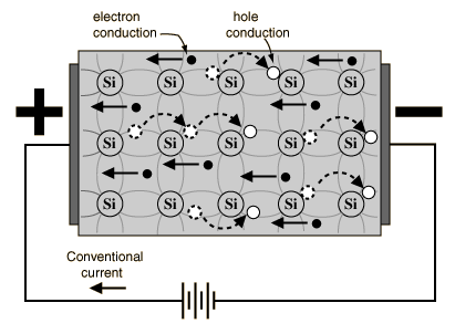
A silicon crystal is different from an insulator because at any temperature above absolute zero temperature, there is a finite probability that an electron in the lattice will be knocked loose from its position, leaving behind an electron deficiency called a "hole".
If a voltage is applied, then both the electron and the hole can contribute to a small current flow.
|
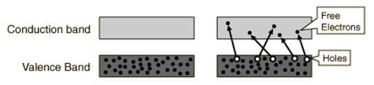
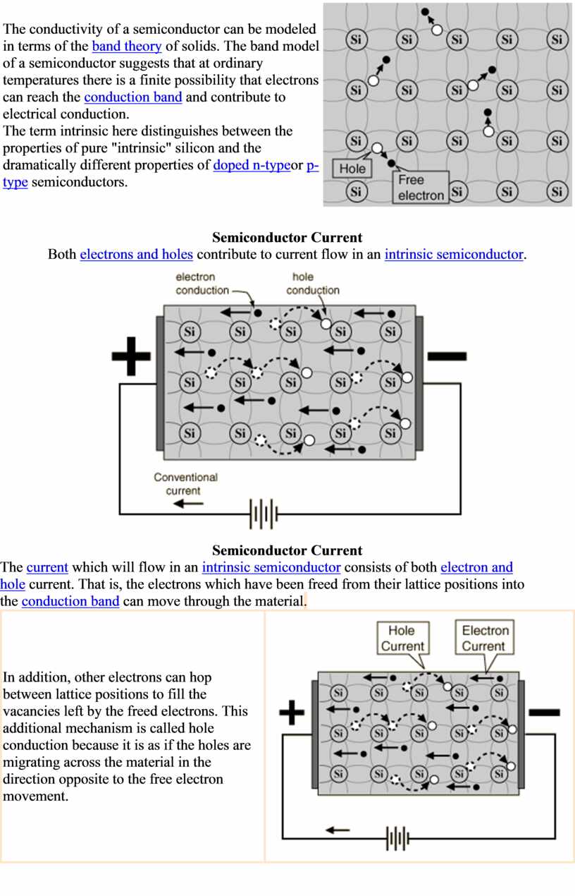
The conductivity of a semiconductor can be modeled in terms of the band theory of solids. The band model of a semiconductor suggests that at ordinary temperatures there is a finite possibility that electrons can reach the conduction band and contribute to electrical conduction. The term intrinsic here distinguishes between the properties of pure "intrinsic" silicon and the dramatically different properties of doped n-typeor p-type semiconductors. |
|
Semiconductor Current
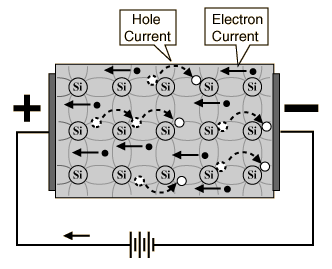
Both electrons and holes contribute to current flow in an intrinsic semiconductor.
Semiconductor Current
The current which will flow in an intrinsic semiconductor consists of both electron and hole current. That is, the electrons which have been freed from their lattice positions into the conduction band can move through the material.
|
In addition, other electrons can hop between lattice positions to fill the vacancies left by the freed electrons. This additional mechanism is called hole conduction because it is as if the holes are migrating across the material in the direction opposite to the free electron movement. |
|
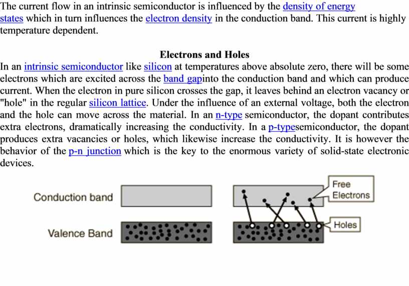
The current flow in an intrinsic semiconductor is influenced by the density of energy states which in turn influences the electron density in the conduction band. This current is highly temperature dependent.
Electrons and Holes
In an intrinsic semiconductor like silicon at temperatures above absolute zero, there will be some electrons which are excited across the band gapinto the conduction band and which can produce current. When the electron in pure silicon crosses the gap, it leaves behind an electron vacancy or "hole" in the regular silicon lattice. Under the influence of an external voltage, both the electron and the hole can move across the material. In an n-type semiconductor, the dopant contributes extra electrons, dramatically increasing the conductivity. In a p-typesemiconductor, the dopant produces extra vacancies or holes, which likewise increase the conductivity. It is however the behavior of the p-n junction which is the key to the enormous variety of solid-state electronic devices.
Скачано с www.znanio.ru
Материалы на данной страницы взяты из открытых источников либо размещены пользователем в соответствии с договором-офертой сайта. Вы можете сообщить о нарушении.