Поделиться

The effect on the photoelectric parameters of non-uniformly light absorption in structures based on a-Si:H
B.F.Ergashev
Namangan State University
B.Ergashev@yahoo.com
Abstract: In this manuscript, conclusions of an analytical expression that determines the dependence of the height of the potential barrier, which was obtained upon unevenly light absorption of over the thickness of the i-layer in the target of video with n-i-p structures based on a-Si: H, on the light intensity were given. Also, it was investigated that the dependence of the width of the space charge region (SCR) on certain features of a-Si: H.
Keywords: Hydrogenated Amorphous Silicon(a-Si: H), the target of Vidicon, tails of Conductive and Valence zones, State density, gap mobility.
Introduction.
Various photoelectric devices had been created based on amorphous hydrogenated silicon, including solar cells, field transistors, memory elements, and badge tubes. In recent years, however, intense research has been carried out to establish and enhance cascade solar cells[1,2,3,4] with a cascade structure based on a-Si: H/μk-Si: H. Given that the total layer in the cascade structure of solar cells is d ~ 6 μm thick, according to Bouguer’s law, I=I0·e-αd Si: H in the layers causes uniform absorption. This case causes to an uneven distribution of photogenerated charges.
In this manuscript, some of the physical processes that appear from the illumination of light has investigated.
Issue and analysis of results.
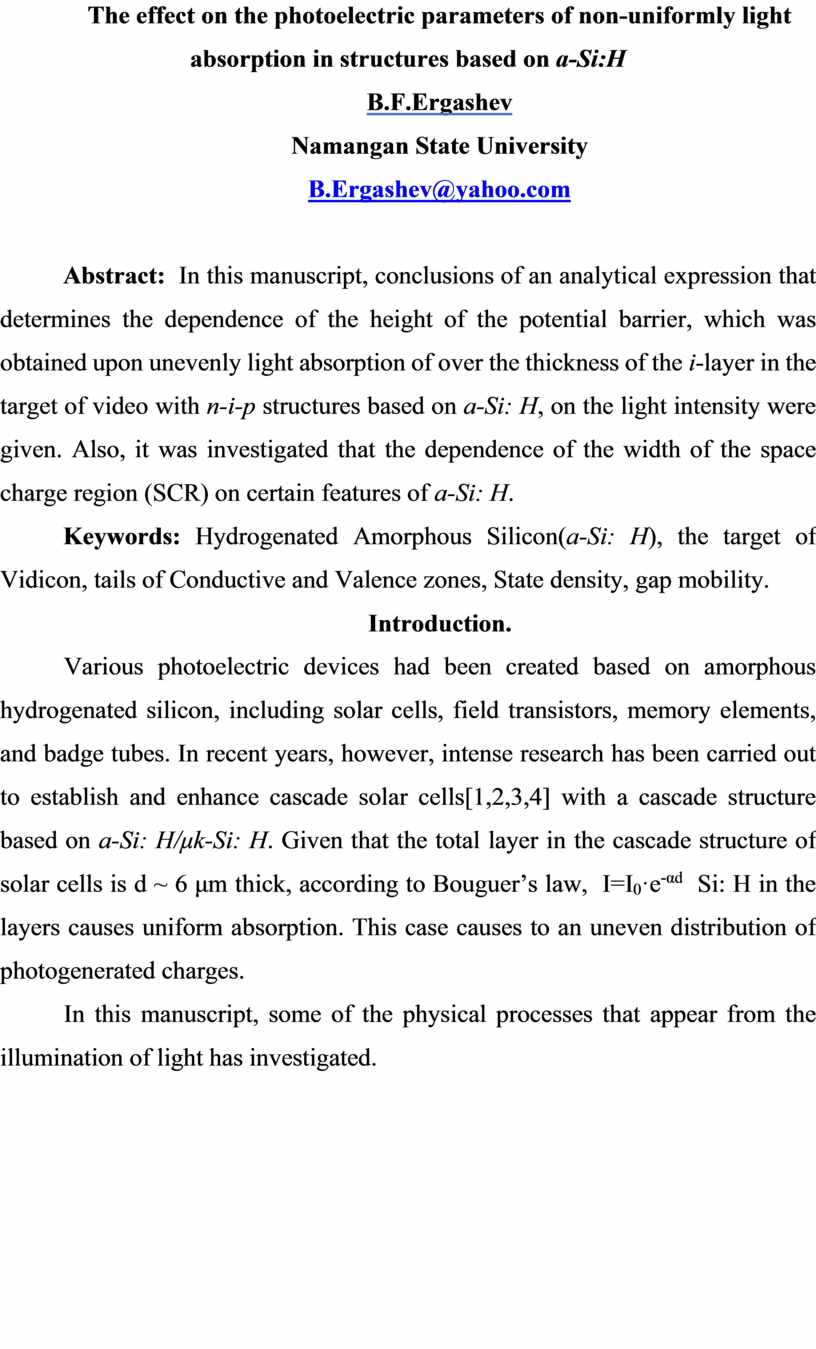
It is known that incident light on the Vidicon target is absorbed by the i-a-Si: H layer at the surface. Therefore, i-a-Si: H forms a reservoir of charges that carry currents in the surface. Figure 1 shows the pre- and post-zone diagrams for illumination of the layers of the vidicon.

Figure 1. Pre- and post-zone diagrams of illumination of the layers of Vidicon target.
The illuminated light absorbs by all the charged states in the i-a-Si: H layer or the free electron and cavity formed interact with the charge states. It is clear that the density of charged conditions of the i-a-Si: H in the slit of motion are as follows.
1. Charge states on the tale of Conductivity and Valence region.
2. In the literature review, for i-a-Si: H, we found that two types of D-centers occur in the recombination process Si: Si That is, D--centers with electronic handles, and D0-centers for holes
With this in mind, we can derive the total charge density in the slope of the motion in the form of the sum of the density states above.
![]()
![]() and
and ![]() - the position densities
of the valence field and the conductive sphere tail are subject to exponential
distribution respectively.
- the position densities
of the valence field and the conductive sphere tail are subject to exponential
distribution respectively.
 (1)
(1)
 (2)
(2)
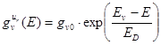
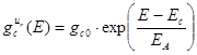
Where gv0 and gc0 are the densities of states above the valence and below the conductivity zones respectively.
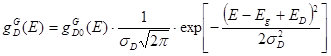
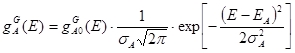
ED and EA are characteristic of cortical energies and receptor levels. As the D-centers are subordinate to the Gaussian distribution, we describe as follows:
 (3)
(3)
 (4)
(4)
Here, ![]() and
and ![]() correspondingly, the Gaussian distribution is the
maximum value for the D-- and D0 -centers.
correspondingly, the Gaussian distribution is the
maximum value for the D-- and D0 -centers.
ED and EA - Energy roles of maximum values.
The σA – D0 – is the energy width of the center distribution and is determined by the energy size Δ = 0.44 eV, which separates the D-- and D0-centers as determined by the experiments [1,2] according to Powell and Phone. Namely:
![]() (5)
(5)
U = 0.2-0.3 eV, D0 and D- - the energy difference between the maximums of the centers After determining the distribution of energy states of a-Si: H in the energy slot, we can estimate the electron (n) and cavity concentration at D- and D0-centers.
But first, we need to explain which Fermi levels shift due to which energy states the charge carriers hold.
As we know, we can omit expressions (1) and (2) because of the presence of holes only in the photoelectric conductance of the vidicon target. Furthermore, considering that gv0 ≈ 1021 сm-3/eV and gA0 ≈ 1018 сm-3/eV in expressions (1) and (4) are not applicable Ev-E << E-EA. The inequality has been fulfilled. Then we can find the Fermi level shift in expression (3) only.
The results of the experiment confirm our experiments’ results above.
In [6,7,8], the authors believe that step-by-step recombination does not occur in the visible spectral range of light at a room temperature of 104 V/сm or higher. Any recombination occurs only in the charge carriers held in one center.
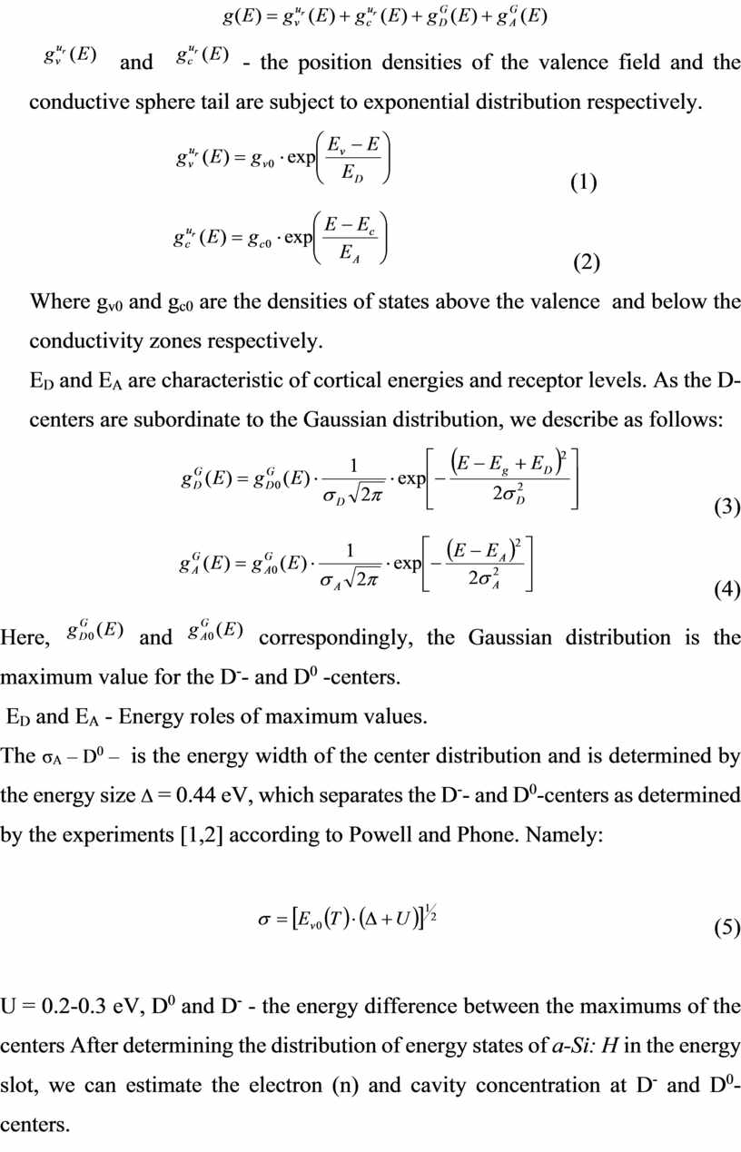
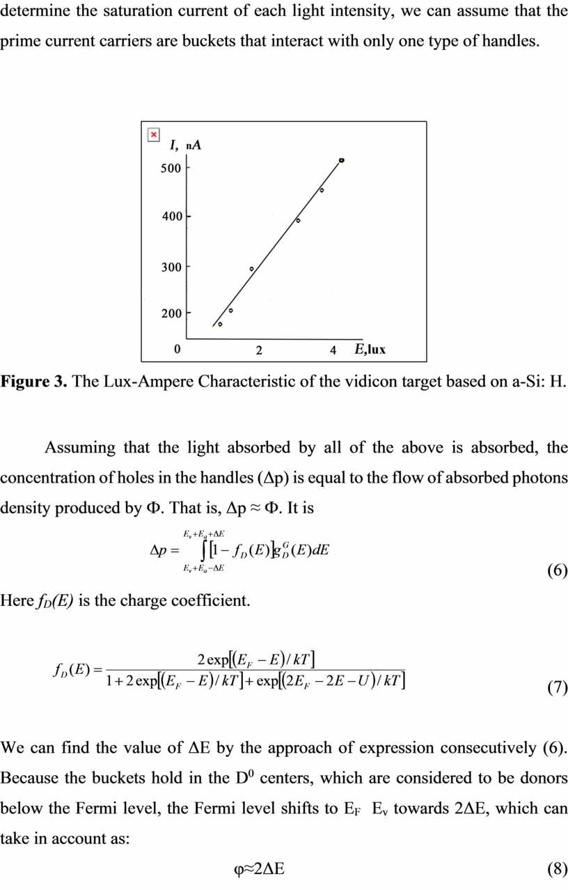
According to the Rose model [9], the Lux-Amper characteristic is linear if non-primary current carriers catches in only one type of handles during their movement.

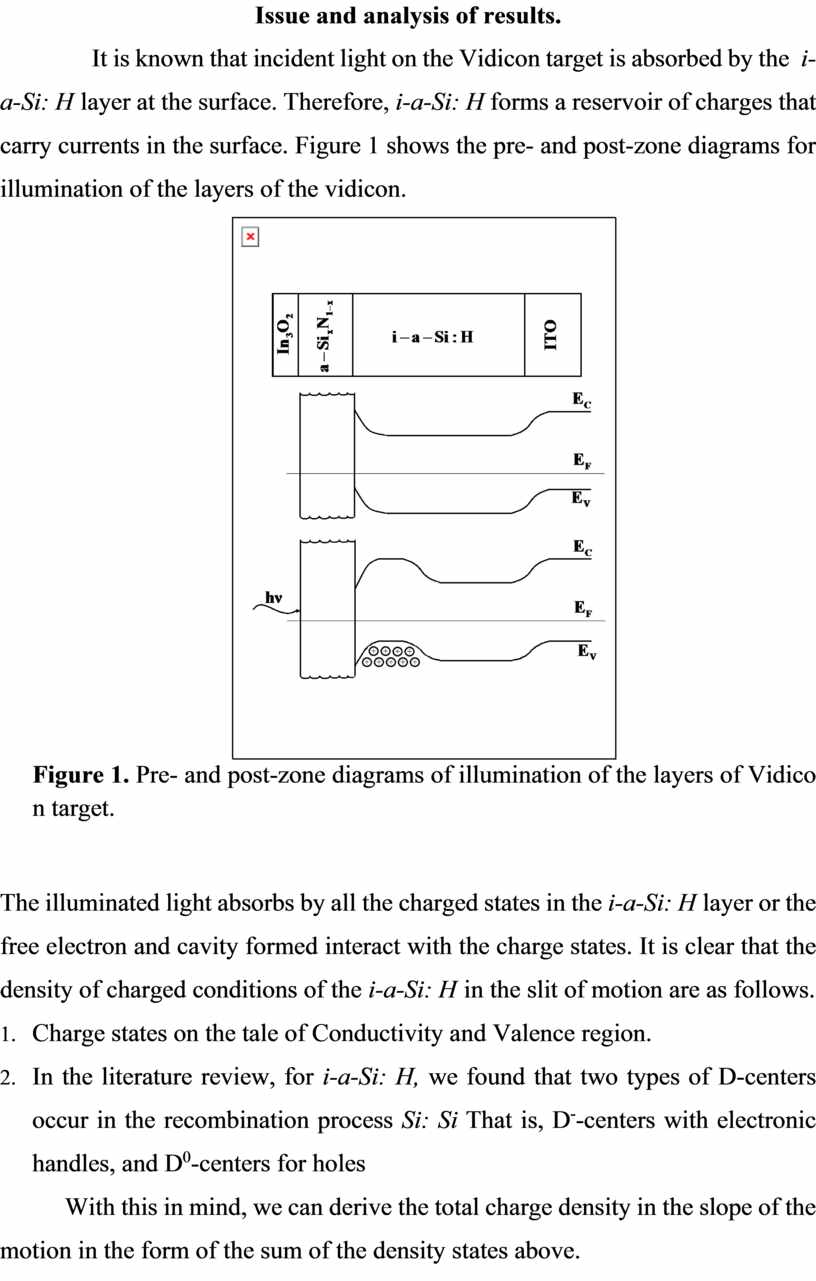
Figure 2. Photo-VACH that is corresponding to the illumination of different intensities.
Figure2 shows the graphics-VACH graphs corresponding to different intensities of illumination. Based on the LACH (Figure3) obtained from the illustration to determine the saturation current of each light intensity, we can assume that the prime current carriers are buckets that interact with only one type of handles.

Figure 3. The Lux-Ampere Characteristic of the vidicon target based on a-Si: H.
Assuming that the light absorbed by all of the above is absorbed, the concentration of holes in the handles (Δp) is equal to the flow of absorbed photons density produced by Ф. That is, Δp ≈ Ф. It is
 (6)
(6)
Here fD(E) is the charge coefficient.
![]() (7)
(7)
We can find the value of ΔE by the approach of expression consecutively (6). Because the buckets hold in the D0 centers, which are considered to be donors below the Fermi level, the Fermi level shifts to EF Ev towards 2ΔE, which can take in account as:
φ≈2ΔE (8)
The concentration of D- and D0 -centers on the mobility rod a-Si: H does not exceed any value. Therefore, the number of photons targeted to the vidicon does not exceed these values. Also, light intensity according to Bouguer’s law.
![]()
exponentially decreases depending on the Then, depending on the intensity, the i-a-Si: H concentration of non-core currents in the absorbed part of the light increases, that is, the pores.
It is well-known that the potential barrier in the case of metal-semiconductor contact of dielectric barriers depends on the width of the charge field on the semiconductor surface. We can calculate the structure of the vidicon sign in the same way because we can dielectrically coat the a-SixN1-x thin layer (thickness ~ 20 nm, Eg = 3.5 eV, ρ = 1014 Оm*m) between the In2O3: Sn layer and the i-a-Si: H layer. If we assume that the surface charge distribution sprays along the axis perpendicular to the surface, the concentration of these surface states decreases by exponential law concerning the semiconductor [2,3].
As we look, the intensity of photogeneration in the deeper layer of
i-a-Si: H increases with increasing light intensity. This rise, in turn, affects the width of the voltage field and the potential for peak voltage. We show the variation of the width of the charge field as follows:
![]() (9)
(9)
![]() - Debai length of
shielding. According to (9), as the light intensity increases, the thickness of
the volume charge field decreases due to the rise in the photogenerated pore
concentration. According to ω ~ ls [4,5], the charge
distribution can be expressed by solving the Poisson equation when the width of
the area of the volume charge is around the order ls. ls is a
characteristic parameter for the exponential reduction of the semiconductor
surface states [2,3].
- Debai length of
shielding. According to (9), as the light intensity increases, the thickness of
the volume charge field decreases due to the rise in the photogenerated pore
concentration. According to ω ~ ls [4,5], the charge
distribution can be expressed by solving the Poisson equation when the width of
the area of the volume charge is around the order ls. ls is a
characteristic parameter for the exponential reduction of the semiconductor
surface states [2,3].
Summary.
Analyzing of the results shows that:
At the Large thicknesses of a-Si: H, uneven light absorption occurs along with the width. Above condition creates a potential barrier in the single layer. The potential barrier causes by the defect states distributed by the Gaussian distribution on the gap mobility of a-Si: H.
According to the Rose model, recombination occurs mainly through single-charge centers. We can use this property for finite modeling of Si: H cascade structural elements.
Bibliography.
1. Spear W. E., Le Comber P. G. Investigation of the Localised distribution in amorphous Si films. //J. None. Cryst. Solids. 1972. Vol. 8-10. p. 727-738.
2. Madon Le Comber P. G., Spear W. E. Investigation of the density of Localised states in a-Si using the field-effect technique. //J. None. Cryst. Solids. 1976. vol. 20. p. 239-257.
3. Amorphous semiconductors: Per. Sang. / Pod. Red. M. Brodski. M.: Mir, 1982. 418 p.
4. Physics of Hydrogenated Silicon; VIP. 1. Structure, development, and devices. Per. Sang. / Pod. Red. J. Djounopoulosa, J. Lukowski. M.: Mir, 1987. 368 p.
5. C. R. Wronski, J. M. Pearce, R. J. Koval, A. S. Ferlauto, and R. W. Collins. Progress in amorphous silicon-based solar cell technology. RIO. 02-World Climate & Energy Event, N1, 2002, p. 67-72.
6. Oda S. et all. J. Appl. Physics, 52, 1981, p. 7275.
7. Tiedje T. et all. Solar Cells, 2, 1980, p.301.
8. Oda S. et all. Philos Mag, 43, 1981, p.1079.
9. A. Hadjadj, N. Pham, P. Roca, I. Cabarrocas, O. Jbara and G. Djellouli
Appl. Phys. 107, 083509, 2010.
Скачано с www.znanio.ru

Материалы на данной страницы взяты из открытых источников либо размещены пользователем в соответствии с договором-офертой сайта. Вы можете сообщить о нарушении.