Поделиться

TASK1 : CURRENT IN METALS https://www.youtube.com/watch?v=7RpyURBNZyU&t=177s
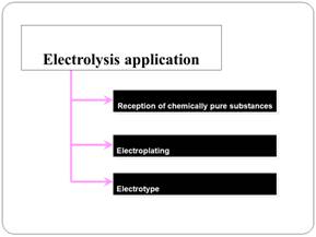
TASK 2: CURRENT IN GASES
Gases consist of neutral molecules, and are, therefore, good insulators. Yet under certain conditions, a breakdown of the insulating property occurs, and current can pass through the gas. Several phenomena are associated with the electric discharge in gases; among them are spark, dark (Townsend) discharge, glow, corona, and arc.
In order to conduct electricity, two conditions are required. First, the normally neutral gas must create charges or accept them from external sources, or both. Second, an electric field should exist to produce the directional motion of the charges. A charged atom or molecule, or ion, can be positive or negative; electrons are negative charges. In electrical devices, an electric field is produced between two electrodes, called anode and cathode, made of conducting materials.
The process of changing a neutral atom or molecule into an ion is called ionization. Ionized gas is called plasma. Conduction in gases is distinguished from conduction in solids and liquids in that the gases play an active role in the process. The gas not only permits free charges to pass though, but itself may produce charges. Cumulative ionization occurs when the original electron and its offspring gain enough energy, so each can produce another electron. When the process is repeated over and over, the resulting process is called an avalanche.
For any gas at a given pressure and temperature there is a certain voltage value, called breakdown potential, that will produce ionization. Application of a voltage above the critical value would initially cause the current to increase due to cumulative ionization, and the voltage is then decreased. If the pressure is not too low, conduction is concentrated into a narrow, illuminated, "spark" channel. By receiving energy from the current, the channel becomes hot and may produce shock-waves. Natural phenomena are the lightning and the associated thunder, that consist of high voltages and currents that cannot be artificially achieved.
An arc can be produced in high pressure following a spark. This occurs when steady conditions are achieved, and the voltage is low but sufficient to maintain the required current. In low pressures, the transient stage of the spark leads to the glow discharge, and an arc can later be formed when the current is further increased. In arcs, the thermionic effect is responsible for the production of free electrons that are emitted from the hot cathode. A strong electric field at the metallic surface lowers the barrier for electron emission, and provides a field emission. Because of the high temperature and the high current involved, however, some of the mechanisms of arcs cannot be easily studied.
Current-voltage curve: A fact detector is made up of conducting material along with an electrically isolated central wire. An extremely thin window made of mylar, aluminium or beryllium is given at one end of the detector that is filled along with a mixture of a primary gas (such as Ar, Kr, Xe termed as P gas) and a quenching gas (such as CH4, alcohol vapours or halogen gas like as Cl2). Alternatively a continuous flow of the gas (liquid petroleum gas is frequent used) could be sent through the chamber. Within that case, it is known as continuous flow proportional counter.
In the absence of any radiation there is no ion-pairs are formed and therefore no current passes through the tube. Therefore, while voltage is applied across the central wire and nuclear radiations enter the tube, ion pairs are formed and current passes. As voltage is rise the number of ion pairs formed increases.
TASK 3: SEMICONDUCTOR DEVICES
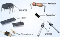
The Semiconductor device is made up of a material that is neither a good conductor nor a good insulator, it is called a semiconductor. Such devices have established wide applications because of their reliability, compactness, and low cost. These are discrete components which are used in power devices, compactness optical sensors, and light emitters, including solid-state lasers. They have a wide range of current and voltage handling capabilities, with current ratings more than 5,000 amperes and voltage ratings more than 100,000 volts. More importantly, semiconductor devices lend themselves to integration into complex but readily build-up microelectronic circuits. They are having probable future, the key elements of the majority of electronic systems including communications with data-processing, consumer, and industrial-control equipment.
 Semiconductor devices are nothing
but electronic components that
exploit the electronic properties of semiconductor materials, like as silicon,
germanium, and gallium arsenide, as well as organic semiconductors.
Semiconductor devices have replaced vacuum tubes in many
applications. They use electronic conduction in the solid state as opposed
to the thermionic emission in a high vacuum. Semiconductor devices are
manufactured for both discrete devices and integrated circuits, which consist of
from a few to billions of devices manufactured and interconnected on a single
semiconductor substrate or wafer.
Semiconductor devices are nothing
but electronic components that
exploit the electronic properties of semiconductor materials, like as silicon,
germanium, and gallium arsenide, as well as organic semiconductors.
Semiconductor devices have replaced vacuum tubes in many
applications. They use electronic conduction in the solid state as opposed
to the thermionic emission in a high vacuum. Semiconductor devices are
manufactured for both discrete devices and integrated circuits, which consist of
from a few to billions of devices manufactured and interconnected on a single
semiconductor substrate or wafer.
Semiconductor Devices
Semiconductor materials are useful by their behavior which can be easily manipulated by the addition of impurities is known as doping. Semiconductor conductivity can be controlled by the electric or magnetic field, by exposure to light or heat, or by the mechanical deformation of a doped mono crystalline grid; thus, semiconductors can make excellent sensors. Current conduction in a semiconductor occurs free of electrons and holes, collectively known as charge carriers. Doping of silicon is done by adding a small amount of impurity atoms and also for phosphorus or boron, significantly increases the number of electrons or holes within the semiconductor.
When a doped semiconductor contains excess holes it is called “p-type”(positive for holes)semiconductor, and when it contains some excess of free electrons, it is known as “n-type”(negative for electrons) semiconductor, is the sign of charge of the majority mobile charge carriers. The junctions which formed where n-type and p-type semiconductors are joined together is called p–n junction.
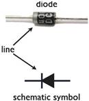 A semiconductor diode is a device typically made
up of a single p-n junction. The junction of a p-type and n-type semiconductor
forms a depletion region where current conduction is reserved by the lack of
mobile charge carriers. When the device is forward biased, this depletion
region is reduced, allowing for significant conduction, when the diode is reverse
biased, the only less current can be achieved and the depletion region can be
extended. Exposing a semiconductor to light can produce electron hole pairs,
which increases the number of free carriers and thereby the conductivity.
Diodes optimized to take advantage of this phenomenon is known as photodiodes.
Compound semiconductor diodes are also being used to generate light,
light-emitting diodes and laser diodes.
A semiconductor diode is a device typically made
up of a single p-n junction. The junction of a p-type and n-type semiconductor
forms a depletion region where current conduction is reserved by the lack of
mobile charge carriers. When the device is forward biased, this depletion
region is reduced, allowing for significant conduction, when the diode is reverse
biased, the only less current can be achieved and the depletion region can be
extended. Exposing a semiconductor to light can produce electron hole pairs,
which increases the number of free carriers and thereby the conductivity.
Diodes optimized to take advantage of this phenomenon is known as photodiodes.
Compound semiconductor diodes are also being used to generate light,
light-emitting diodes and laser diodes.
The silicon (Si) is most widely used material in semiconductor devices. It’s having lower raw material cost and relatively simple process. Its useful temperature range makes it currently the best compromise among the various competing materials. Silicon used in semiconductor device manufacturing is presently fabricated into bowls that are large enough in diameter to allow the manufacture of 300 mm (12 in.) wafers.
Germanium (Ge) was a widely used in early semiconductor material, but its thermal sensitivity makes less useful than silicon. Nowadays, germanium is often alloyed with (Si) silicon for use in very-high-speed SiGe devices; IBM is a main producer of such devices.
Gallium arsenide (GaAs) is also widely used with high-speed devices, but so far, it has been difficult to form large-diameter bowls of this material, limiting the wafer diameter sizes significantly smaller than silicon wafers thus making mass production of Gallium arsenide (GaAs) devices significantly more expensive than silicon.
All types of transistor can be used as the building blocks of logic gates, which is useful to design of digital circuits. In digital circuits like as microprocessors, transistors so which is acting as a switch (on-off); in the MOSFET, for example, the voltage applied to the gate determines whether the switch is on or off.
The transistors are used for analog circuits do not act as switches (on-off); relatively, they respond to a continuous range of input with a continuous range of output. Common analog circuits include oscillators and amplifiers. The circuits that interface or translate between analog circuits and digital circuits are known as the mixed-signal circuits.
· As semiconductor devices have no filaments, hence no power is needed to heat them to cause the emission of electrons.
· Since no heating is required, semiconductor devices are set into operation as soon as the circuit is switched on.
· During operation, semiconductor devices do not produce any humming noise.
· Semiconductor devices require low voltage operation as compared to vacuum tubes.
· Owing to their small sizes, the circuits involving semiconductor devices are very compact.
· Semiconductor devices are shock proof.
· Semiconductor devices are cheaper as compared to vacuum tubes.
· Semiconductor devices have an almost unlimited life.
· As no vacuum has to be created in semiconductor devices, they have no vacuum deterioration trouble.
· The noise level is higher in semiconductor devices as compared to that in the vacuum tubes.
· Ordinary semiconductor devices cannot handle as more power as ordinary vacuum tubes can do.
· In high frequency range, they have poor responder.
Thus, this is all about different types of semiconductor devices include two terminals, three terminals and four terminal devices. We hope that you have got a better understanding of this concept. Furthermore, any doubts regarding this concept or electrical and electronic projects, please give your feedback by commenting in the comment section below. Here is a question for you, what are the applications of semiconductor devices?
https://www.youtube.com/watch?v=1eqMwZ6qCCs
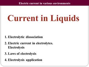
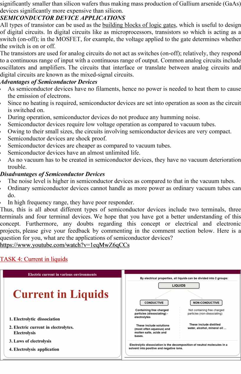
TASK 4: Current in liquids
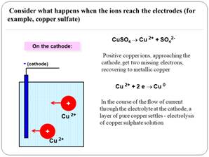
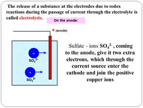
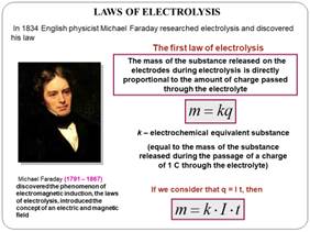
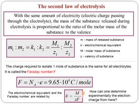
|
|
|
|
|
|
|
|
|
|
|
|
|
|
|
|
|
|
|
https://www.youtube.com/watch?v=7uIIq_Ofzgw |
|
|
|
|
Скачано с www.znanio.ru


Материалы на данной страницы взяты из открытых источников либо размещены пользователем в соответствии с договором-офертой сайта. Вы можете сообщить о нарушении.