Поделиться

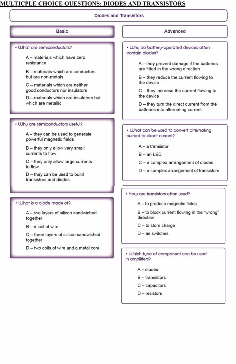
MULTICPLE CHOICE QUESTIONS: DIODES AND TRANSISTORS
READING TASK: THE SEMI-CONDUCTOR DIODE
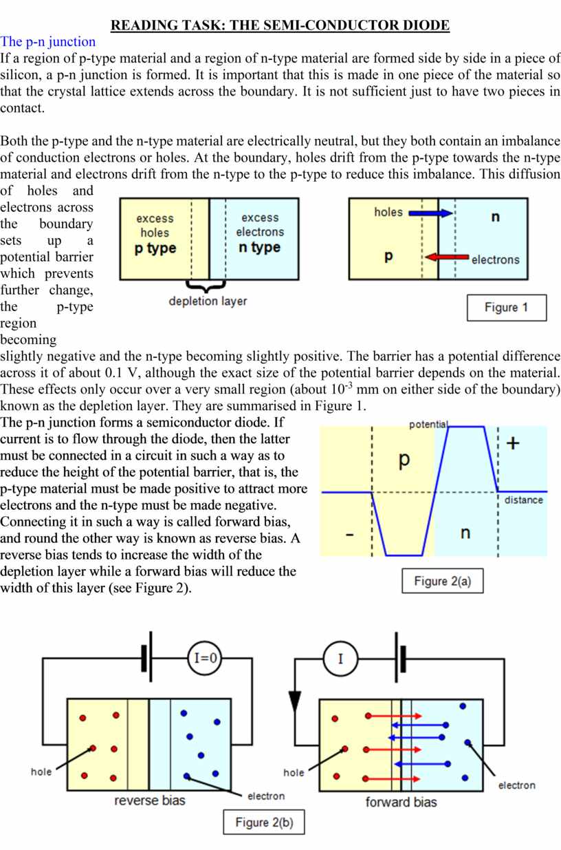
The p-n junction
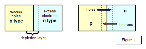 If a region of p-type material and a region of n-type material are
formed side by side in a piece of silicon, a p-n junction is formed. It is
important that this is made in one piece of the material so that the crystal
lattice extends across the boundary. It is not sufficient just to have two
pieces in contact.
If a region of p-type material and a region of n-type material are
formed side by side in a piece of silicon, a p-n junction is formed. It is
important that this is made in one piece of the material so that the crystal
lattice extends across the boundary. It is not sufficient just to have two
pieces in contact.
Both the p-type and the n-type material are electrically neutral, but they both
contain an imbalance of conduction electrons or holes. At the boundary, holes
drift from the p-type towards the n-type material and electrons drift from the
n-type to the p-type to reduce this imbalance. This diffusion of holes and
electrons across the boundary sets up a potential barrier which prevents
further change, the p-type region becoming slightly negative and the n-type
becoming slightly positive. The barrier has a potential difference across it of
about 0.1 V, although the exact size of the potential barrier depends on the
material. These effects only occur over a very small region (about 10-3 mm
on either side of the boundary) known as the depletion layer. They are
summarised in Figure 1.
 The p-n junction forms a semiconductor diode. If current is to
flow through the diode, then the latter must be connected in a circuit in such
a way as to reduce the height of the potential barrier, that is, the p-type
material must be made positive to attract more electrons and the n-type must be
made negative.
The p-n junction forms a semiconductor diode. If current is to
flow through the diode, then the latter must be connected in a circuit in such
a way as to reduce the height of the potential barrier, that is, the p-type
material must be made positive to attract more electrons and the n-type must be
made negative.
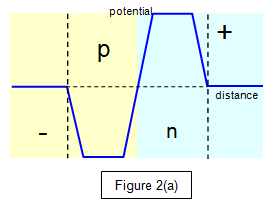
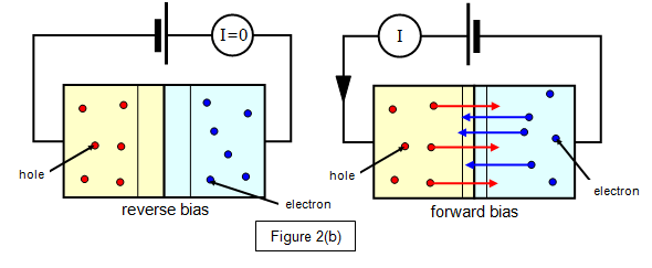
Connecting it in such a way is called forward bias, and round the other way is
known as reverse bias. A reverse bias tends to increase the width of the
depletion layer while a forward bias will reduce the width of this layer (see
Figure 2).
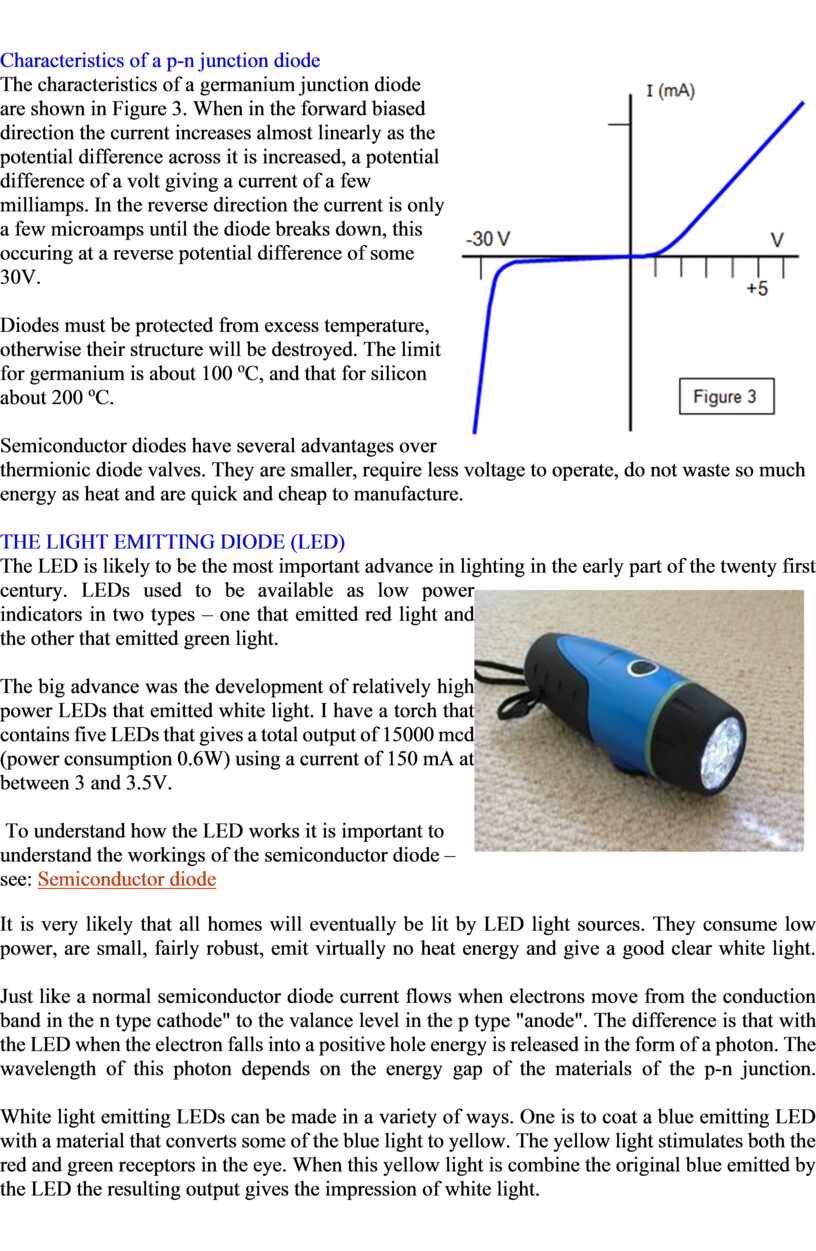
Characteristics of a p-n junction diode
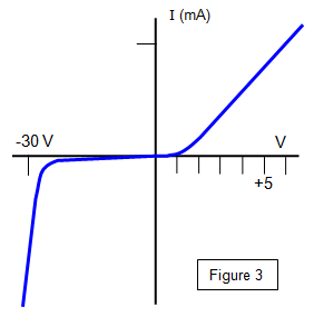 The characteristics of a germanium junction diode are shown in
Figure 3. When in the forward biased direction the current increases almost
linearly as the potential difference across it is increased, a potential difference
of a volt giving a current of a few milliamps. In the reverse direction the
current is only a few microamps until the diode breaks down, this occuring at a
reverse potential difference of some 30V.
The characteristics of a germanium junction diode are shown in
Figure 3. When in the forward biased direction the current increases almost
linearly as the potential difference across it is increased, a potential difference
of a volt giving a current of a few milliamps. In the reverse direction the
current is only a few microamps until the diode breaks down, this occuring at a
reverse potential difference of some 30V.
Diodes must be protected from excess temperature, otherwise their structure
will be destroyed. The limit for germanium is about 100 oC, and
that for silicon about 200 oC.
Semiconductor diodes have several advantages over thermionic diode valves. They
are smaller, require less voltage to operate, do not waste so much energy as
heat and are quick and cheap to manufacture.
THE LIGHT EMITTING DIODE (LED)
The LED is likely to be the
most important advance in lighting in the early part of the twenty first
century. LEDs used to be available as low power indicators in two types – one
that emitted 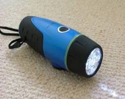 red light and the other that emitted green light.
The big advance was the development of relatively high power LEDs that emitted white light. I have a torch that contains five LEDs that gives a total output of 15000 mcd (power consumption 0.6W) using a current of 150 mA at between 3 and 3.5V.
To understand how the LED works it is important to understand the
workings of the semiconductor diode – see: Semiconductor diode
It is very likely that all homes
will eventually be lit by LED light sources. They consume low power, are small,
fairly robust, emit virtually no heat energy and give a good clear white light.
Just like a normal semiconductor diode current flows when electrons move from
the conduction band in the n type cathode" to the valance level in the p
type "anode". The difference is that with the LED when the electron
falls into a positive hole energy is released in the form of a photon. The
wavelength of this photon depends on the energy gap of the materials of the p-n
junction.
White light emitting LEDs can be made in a variety of ways. One is to coat a
blue emitting LED with a material that converts some of the blue light to
yellow. The yellow light stimulates both the red and green receptors in the
eye. When this yellow light is combine the original blue emitted by the LED the
resulting output gives the impression of white light.
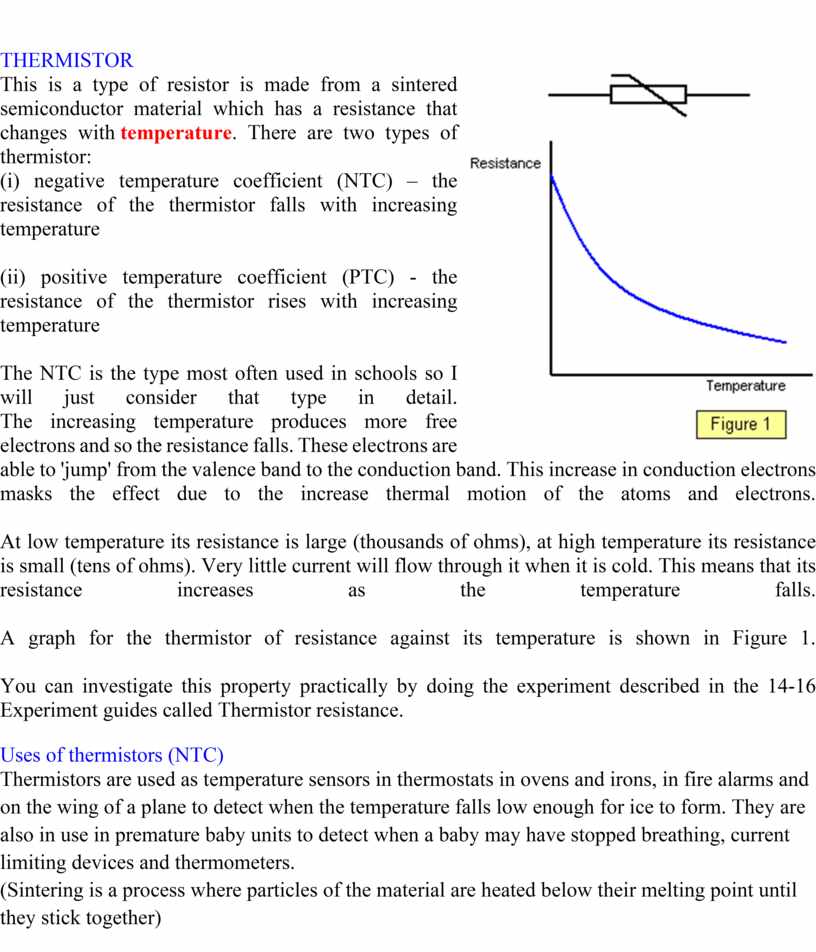
THERMISTOR
 This is a type of resistor is made from a sintered semiconductor
material which has a resistance that changes with temperature. There are two types of
thermistor:
This is a type of resistor is made from a sintered semiconductor
material which has a resistance that changes with temperature. There are two types of
thermistor:
(i) negative temperature coefficient (NTC) – the resistance of the thermistor
falls with increasing temperature
(ii) positive temperature coefficient (PTC) - the resistance of the thermistor
rises with increasing temperature
The NTC is the type most often used in schools so I will just consider that
type in detail.
The increasing temperature produces more free electrons and so the resistance
falls. These electrons are able to 'jump' from the valence band to the
conduction band. This increase in conduction electrons masks the effect due to
the increase thermal motion of the atoms and electrons.
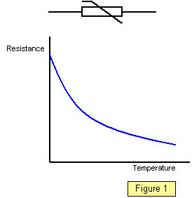
At low temperature its resistance is large (thousands of ohms), at high
temperature its resistance is small (tens of ohms). Very little current will
flow through it when it is cold. This means that its resistance increases as
the temperature falls.
A graph for the thermistor of resistance against its temperature is shown in
Figure 1.
You can investigate this property practically by doing the experiment described
in the 14-16 Experiment guides called Thermistor resistance.
Uses of thermistors (NTC)
Thermistors
are used as temperature sensors in thermostats in ovens and irons, in fire
alarms and on the wing of a plane to detect when the temperature falls low
enough for ice to form. They are also in use in premature baby units to detect
when a baby may have stopped breathing, current limiting devices and
thermometers.
(Sintering is a process where particles of the
material are heated below their melting point until they stick together)
Скачано с www.znanio.ru
Материалы на данной страницы взяты из открытых источников либо размещены пользователем в соответствии с договором-офертой сайта. Вы можете сообщить о нарушении.